PH3259 deals with the semester II B.E Robotics and Automation Syllabus at Anna University based on regulation 2021. In this article, we discuss the applied materials science syllabus along with textbooks and references.
We intend to provide a full-planned syllabus for students to gain knowledge of the syllabus. It will give students to be equipped with perfect books and the required knowledge to prepare for the examinations. These are necessary to get a qualified certificate from the university with aggregate marks. Students must perform well to take a step forward toward their careers. They must earn a qualified degree help them to achieve success in their goals. In this article, PH3259 – Applied Materials Science Syllabus will pioneer the way to do that. Hope the following information is useful. Don’t forget to share it with your classmates.
If you want to know more about the syllabus of B.E Robotics and Automation connected to an affiliated institution’s four-year undergraduate degree program. We provide you with a detailed Year-wise, semester-wise, and Subject-wise syllabus in the following link B.E Robotics and Automation Syllabus Anna University, Regulation 2021.
Aim Of Objectives:
- To make the students understand the basics of crystallography and its importance in studying materials properties.
- To inculcate the knowledge of phase relationships for the understanding of material properties.
- To understand the electrical properties of materials including free electron theory, applications of quantum mechanics, and magnetic materials.
- To instill knowledge on the physics of semiconductors, determination of charge carriers, and device applications.
- To establish a sound grasp of knowledge on different optical properties of materials, optical displays, and applications.
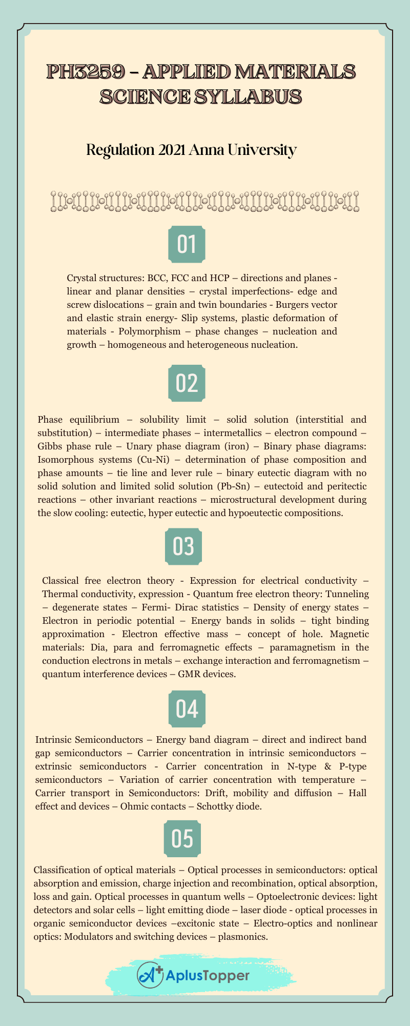
PH3259 – Applied Materials Science Syllabus
Unit I: Crystallography
Crystal structures: BCC, FCC and HCP – directions and planes – linear and planar densities – crystal imperfections- edge and screw dislocations – grain and twin boundaries – Burgers vector and elastic strain energy- Slip systems, plastic deformation of materials – Polymorphism – phase changes – nucleation and growth – homogeneous and heterogeneous nucleation.
Unit II: Phase Diagrams
Phase equilibrium – solubility limit – solid solution (interstitial and substitution) – intermediate phases – intermetallics – electron compound – Gibbs phase rule – Unary phase diagram (iron) – Binary phase diagrams: Isomorphous systems (Cu-Ni) – determination of phase composition and phase amounts – tie line and lever rule – binary eutectic diagram with no solid solution and limited solid solution (Pb-Sn) – eutectoid and peritectic reactions – other invariant reactions – microstructural development during the slow cooling: eutectic, hyper eutectic and hypoeutectic compositions.
Unit III: Electrical And Magnetic Properties Of Materials
Classical free electron theory – Expression for electrical conductivity – Thermal conductivity, expression – Quantum free electron theory: Tunneling – degenerate states – Fermi- Dirac statistics – Density of energy states – Electron in periodic potential – Energy bands in solids – tight binding approximation – Electron effective mass – concept of hole. Magnetic materials: Dia, para and ferromagnetic effects – paramagnetism in the conduction electrons in metals – exchange interaction and ferromagnetism – quantum interference devices – GMR devices.

Unit IV: Semiconductors And Transport Physics
Intrinsic Semiconductors – Energy band diagram – direct and indirect band gap semiconductors – Carrier concentration in intrinsic semiconductors – extrinsic semiconductors – Carrier concentration in N-type & P-type semiconductors – Variation of carrier concentration with temperature – Carrier transport in Semiconductors: Drift, mobility and diffusion – Hall effect and devices – Ohmic contacts – Schottky diode.
Unit V: Optical Properties Of Materials
Classification of optical materials – Optical processes in semiconductors: optical absorption and emission, charge injection and recombination, optical absorption, loss and gain. Optical processes in quantum wells – Optoelectronic devices: light detectors and solar cells – light emitting diode – laser diode – optical processes in organic semiconductor devices –excitonic state – Electro-optics and nonlinear optics: Modulators and switching devices – plasmonics.
Text Books:
- V. Raghavan. Materials Science and Engineering: A First Course, Prentice Hall India Learning Private Limited, 2015.
- Safa Kasap, Principles of Electronic Materials and Devices, McGraw Hill, 2018.
- Jasprit Singh, Semiconductor Devices: Basic Principles, Wiley (India), 2007.
- Jasprit Singh, Semiconductor Optoelectronics: Physics and Technology, Mc-Graw Hill India (2019)
- Safa kasap, Optoelectronics & Photonics: Principles and Practices, Pearson, 2013.
References:
- R. Balasubramaniam, Callister’s Materials Science and Engineering. Wiley (Indian Edition), 2014.
- Wendelin Wright and Donald Askeland, Essentials of Materials Science and Engineering, CL Engineering, 2013.
- Robert F.Pierret, Semiconductor Device Fundamentals, Pearson, 2006.
- Simon Sze and Ming-kwei Lee, Semiconductor Devices: Physics and Technology, Wiley, 2015.
- Pallab Bhattacharya, Semiconductor Optoelectronic Devices, Pearson, 2017.
Related Posts On Semester – II:
- HS3252 Professional English – II
- MA3251 Statistics and Numerical Methods
- GE3251 Engineering Graphics
- GE3252 தமிரு் ததொழி்நு்பமு் /Tamils and Technology
Also Visit:
